- 您现在的位置:买卖IC网 > Sheet目录2000 > IDTCV136PAG (IDT, Integrated Device Technology Inc)IC FLEXPC CLK ATI RS400 56-TSSOP
COMMERCIALTEMPERATURERANGE
10
IDTCV136
PROGRAMMABLEFLEXPC CLOCKFORATIRS400
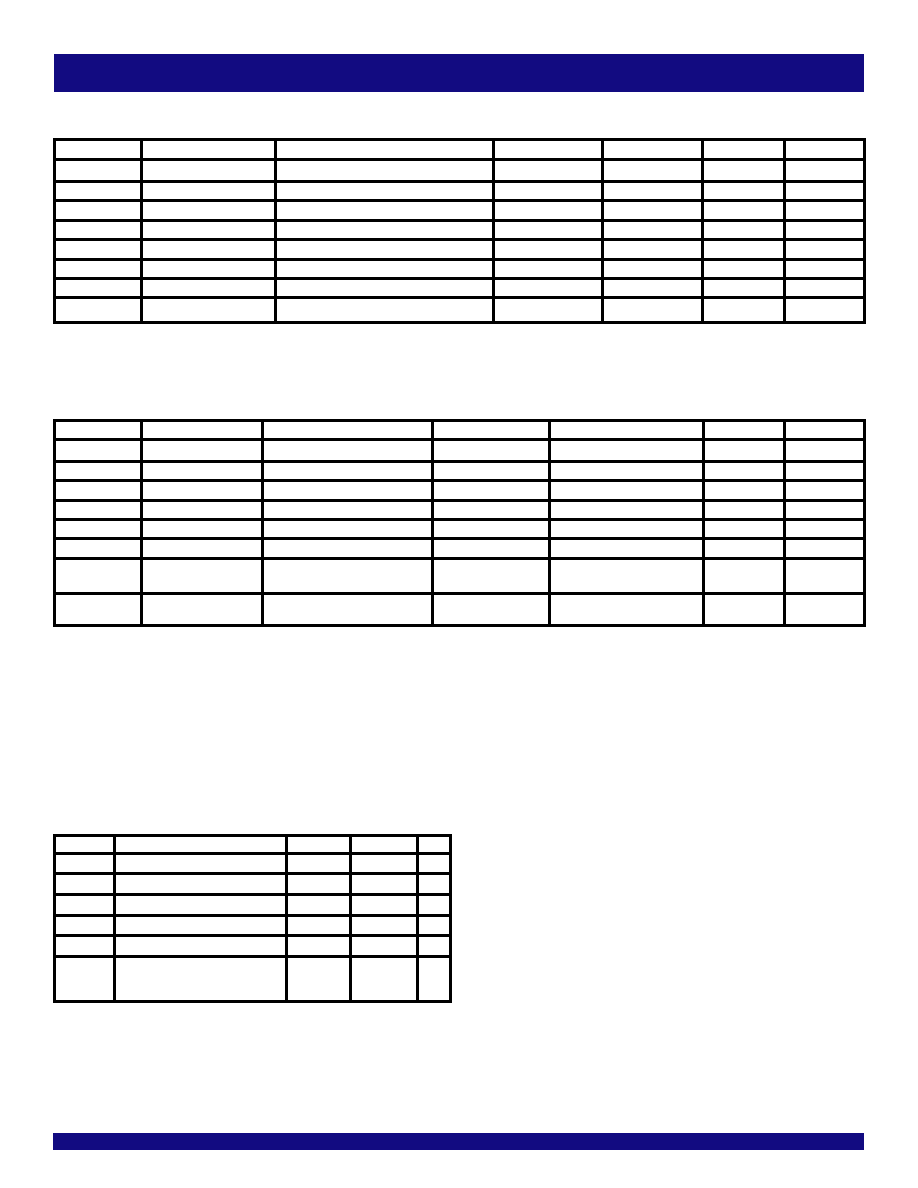
BYTE 21
Bit
Output(s) Affected
Description / Function
0
1
Type
Power On
7
409_410#
R
409_410#
6
FSC latched value on power up
R
FSC
5
FSB latched value on power up
R
FSB
4
FSA latched value on power up
R
FSA
3
Reserved
RW
0
2
Reserved
RW
0
1
Test_scl
On chip test mode Enable
normal
SCLK=1, CLK outputs=1
RW
0
SCLK=0, CLK outputs=0
0
Test_hiz
CLK Outputs Enable
normal
CLK outputs=Tristate
RW
0
BYTE 62 = 60h
BYTE 63 = 13h
BYTE 20 (RESERVED FOR USER)
Bit
Output(s) Affected
Description / Function
0
1
Type
Power On
7
RW
0
6
RW
0
5
RW
0
4
RW
0
3
RW
0
2
RW
0
1
RW
0
RW
0
Symbol
Description
Min
Max
Unit
VDDA
3.3V Core Supply Voltage
4.6
V
VDD
3.3V I/O Supply Voltage
4.6
V
VIH
3.3V Input HIGH
4.6
V
VID
3.3V Input LOW
–0.5
V
TS
Storage Temperature
–65
+150
° C
ESD Prot
Input ESD Protection
2000
V
Human Body Model
ABSOLUTE MAXIMUM RATINGS(1)
NOTE:
1. Stresses greater than those listed under ABSOLUTE MAXIMUM RATINGS may cause
permanent damage to the device. This is a stress rating only and functional operation
of the device at these or any other conditions above those indicated in the operational
sections of this specification is not implied. Exposure to absolute maximum rating
conditions for extended periods may affect reliability.
发布紧急采购,3分钟左右您将得到回复。
相关PDF资料
IDTCV137PAG
IC FLEXPC CLK AMD K8 56-TSSOP
IDTCV142PAG
IC FLEXPC CLK PROGR P4 56-TSSOP
IDTCV146PVG
IC FLEXPC CLK PROGR P4 56-SSOP
IDTCV149PAG
IC FLEXPC CLK PROGR K8 56-TSSOP
IDTNW6005ASG
IC CALLER ID DECODER 20SOIC
IDTNW6006AS
IC CALLER ID DECODER 20-SOIC
IDTSSTE32882HLBBKG
IC REGISTERING CLK DRIVER 176BGA
IDTSSTE32882KA1AKG
IC REGISTERING CLK DRIVER 176BGA
相关代理商/技术参数
IDTCV136PAG8
功能描述:IC FLEXPC CLK ATI RS400 56-TSSOP RoHS:是 类别:集成电路 (IC) >> 时钟/计时 - 专用 系列:FlexPC™, PCI Express® (PCIe) 标准包装:28 系列:- 类型:时钟/频率发生器 PLL:是 主要目的:Intel CPU 服务器 输入:时钟 输出:LVCMOS 电路数:1 比率 - 输入:输出:3:22 差分 - 输入:输出:无/是 频率 - 最大:400MHz 电源电压:3.135 V ~ 3.465 V 工作温度:0°C ~ 85°C 安装类型:表面贴装 封装/外壳:64-TFSOP (0.240",6.10mm 宽) 供应商设备封装:64-TSSOP 包装:管件
IDTCV137PAG
功能描述:IC FLEXPC CLK AMD K8 56-TSSOP RoHS:是 类别:集成电路 (IC) >> 时钟/计时 - 专用 系列:FlexPC™, PCI Express® (PCIe) 标准包装:1,500 系列:- 类型:时钟缓冲器/驱动器 PLL:是 主要目的:- 输入:- 输出:- 电路数:- 比率 - 输入:输出:- 差分 - 输入:输出:- 频率 - 最大:- 电源电压:3.3V 工作温度:0°C ~ 70°C 安装类型:表面贴装 封装/外壳:28-SSOP(0.209",5.30mm 宽) 供应商设备封装:28-SSOP 包装:带卷 (TR) 其它名称:93786AFT
IDTCV137PAG8
功能描述:IC FLEXPC CLK AMD K8 56-TSSOP RoHS:是 类别:集成电路 (IC) >> 时钟/计时 - 专用 系列:FlexPC™, PCI Express® (PCIe) 标准包装:28 系列:- 类型:时钟/频率发生器 PLL:是 主要目的:Intel CPU 服务器 输入:时钟 输出:LVCMOS 电路数:1 比率 - 输入:输出:3:22 差分 - 输入:输出:无/是 频率 - 最大:400MHz 电源电压:3.135 V ~ 3.465 V 工作温度:0°C ~ 85°C 安装类型:表面贴装 封装/外壳:64-TFSOP (0.240",6.10mm 宽) 供应商设备封装:64-TSSOP 包装:管件
IDTCV140
制造商:IDT 制造商全称:Integrated Device Technology 功能描述:PROGRAMMABLE FLEXPC CLOCK FOR P4 PROCESSOR
IDTCV141PAG
功能描述:IC CLK BUFFER 1-8 DIFF 48-TSSOP RoHS:是 类别:集成电路 (IC) >> 时钟/计时 - 专用 系列:- 标准包装:1 系列:- 类型:时钟/频率发生器,多路复用器 PLL:是 主要目的:存储器,RDRAM 输入:晶体 输出:LVCMOS 电路数:1 比率 - 输入:输出:1:2 差分 - 输入:输出:无/是 频率 - 最大:400MHz 电源电压:3 V ~ 3.6 V 工作温度:0°C ~ 85°C 安装类型:表面贴装 封装/外壳:16-TSSOP(0.173",4.40mm 宽) 供应商设备封装:16-TSSOP 包装:Digi-Reel® 其它名称:296-6719-6
IDTCV141PAG8
功能描述:IC CLK BUFFER 1-8 DIFF 48-TSSOP RoHS:是 类别:集成电路 (IC) >> 时钟/计时 - 专用 系列:- 标准包装:28 系列:- 类型:时钟/频率发生器 PLL:是 主要目的:Intel CPU 服务器 输入:时钟 输出:LVCMOS 电路数:1 比率 - 输入:输出:3:22 差分 - 输入:输出:无/是 频率 - 最大:400MHz 电源电压:3.135 V ~ 3.465 V 工作温度:0°C ~ 85°C 安装类型:表面贴装 封装/外壳:64-TFSOP (0.240",6.10mm 宽) 供应商设备封装:64-TSSOP 包装:管件
IDTCV141PVG
功能描述:IC CLK BUFFER 1-8 DIFF 48-SSOP RoHS:是 类别:集成电路 (IC) >> 时钟/计时 - 专用 系列:- 标准包装:28 系列:- 类型:时钟/频率发生器 PLL:是 主要目的:Intel CPU 服务器 输入:时钟 输出:LVCMOS 电路数:1 比率 - 输入:输出:3:22 差分 - 输入:输出:无/是 频率 - 最大:400MHz 电源电压:3.135 V ~ 3.465 V 工作温度:0°C ~ 85°C 安装类型:表面贴装 封装/外壳:64-TFSOP (0.240",6.10mm 宽) 供应商设备封装:64-TSSOP 包装:管件
IDTCV141PVG8
功能描述:IC CLK BUFFER 1-8 DIFF 48-SSOP RoHS:是 类别:集成电路 (IC) >> 时钟/计时 - 专用 系列:- 标准包装:28 系列:- 类型:时钟/频率发生器 PLL:是 主要目的:Intel CPU 服务器 输入:时钟 输出:LVCMOS 电路数:1 比率 - 输入:输出:3:22 差分 - 输入:输出:无/是 频率 - 最大:400MHz 电源电压:3.135 V ~ 3.465 V 工作温度:0°C ~ 85°C 安装类型:表面贴装 封装/外壳:64-TFSOP (0.240",6.10mm 宽) 供应商设备封装:64-TSSOP 包装:管件